Graphene: SuperMaterial
Graphene, a one-atom thick sheet of hexagonally arranged carbon, has existed in theory for the better part of a century, but until 2004 accepted wisdom in the physics and chemistry communities was that theory was as far as graphene was destined to evolve. However in 2004 two scientists, Andre Geim and Konstantin Novoselov, both of whom would later receive the Nobel Prize for their work, overturned conventional wisdom, producing the material in a lab with a very non-lab-like process involving Scotch tape and graphite (pencil lead).
Since the discovery, research on graphene has exploded. It has been a primary or subordinate subject in over 100,000 academic papers, and as of September, 2012, over 2000 patents involving the material have been applied for or awarded.

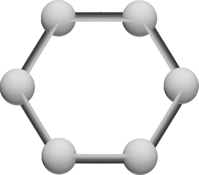
The hexagonal structure of a 6-way bond between carbon atoms -- trillions of which make up a tiny sheet of graphene.

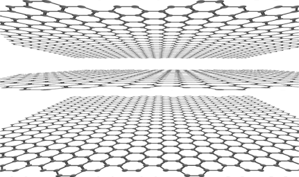
:A visual depiction of the structure of a layered, microscopic segment of graphene. At approximately 200 times stronger than structural steel, given enough layers, graphene would be both harder and stronger than any material ever created, opening the possibility for products and structures that are a fraction of the weight and an exponent of the strength of any existing currently.
The attention surrounding the research has been likened to a gold rush, and it has generated more interest commercially than any material since silicon.
Graphene is extraordinarily strong (the strongest material ever known or tested), supernaturally light, and electrically super-conductive. Its flexibility and structure also make it the leading candidate as the primary component of next-generation, ultra-high speed circuitry in everything from computers, to smartphones, to televisions. It is therefore of interest to a range of industries.
The question, ultimately, isn't if graphene will change everything from computing to manufacturing, but how and when.
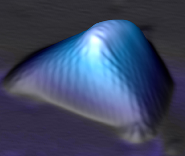
Photo: NewsCenter: Lawrence Berkely National Laboratory
Using microscopy, researchers at Berkely demonstrated that,
by putting a strain on graphene, pseudo-magnetic fields
could be created, stronger than any ever generated in a lab.
On many fronts researchers are still years or decades away from the breakthroughs that will allow a full utilization of graphene, but on some, the future is now, and companies like IBM have already successfully incorporated graphene into working components of commercially viable products.

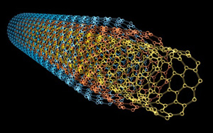
:Rolled sheets of graphene form hyper-conductive carbon nanotubes. These nanotubes work around the primary limiting factor in microchip processing speed by taking chip architecture into the third dimension. There is a lower limit on the size of the essentially flat transistors that make up silicon-based microchips -- the devices that allow information processing in everything from phones to computers. Graphene, carbon nanotubes can effectively stack transistors on top of one another on microchips, allowing for exponentially more transistors on a chip without increasing the size. More transistors means more operations per second, which means more processing power and faster processing speeds.
In this episode of Nova, David Pogue visits Intel and IBM to talk about why carbon nanotubes are the jumping off point in a new age of microchip architecture. The discussion about circuitry begins around 12:30
Understanding the Scale of One-Atom Thick Graphene
This neat little tool is a great way to try to wrap your head around the scale of things that are difficult to put into perspective -- from graphene/carbon nanotubes to the universe: http://scaleofuniverse.com/ This is also a helpful way for parents or teachers to help children understand things that are really difficult to put into words.
To view the scale of a carbon nanotube, press start and begin moving the slider to the left. You'll find the nanotubes around the same size as a phospholipid or glucose molecule -- a few hundred times smaller than the HIV virus and smaller than even one strand of DNA! Also smaller than the smallest thing visible in an optical microscope.
References and Resources
- http://www.nytimes.com/2010/10/06/science/06nobel.html?adxnnl=1&adxnnlx=1348745445-65d1dnUrqVL/vX7TIB3Klw :An article about the Nobel awarded for work completed by Andre Geim and Konstantin Novoselov on graphene
- http://engineering.columbia.edu/graphene-confirmed-strongest-material :Researchers at Columbia demonstrate that graphene is the strongest material ever tested, commenting that a sheet the thickness of saran wrap could support the weight of an elephant, balanced on a pencil
- http://www.nytimes.com/2011/06/10/technology/10chip.html :IBM creates what might be the first commercially viable, graphene based chip
- http://www.nature.com/nature/journal/v448/n7152/abs/nature06016.html :Researchers test graphene's strength and other properties
- http://newscenter.lbl.gov/news-releases/2010/07/29/graphene-under-strain/ :Berkeley scientists test graphene's psuedo-magnetic properties Also See:
- Science 321, 385 (2008); Changgu Lee et al. -- Measurement of the Elastic Properties and Intrinsic Strength of Monolayer Graphene
- Nature: Materials | VOL 6 | MARCH 2007 | www.nature.com/naturematerials -- "The Rise of Graphene" A. K. GEIM AND K. S. NOVOSELOV
Manchester Centre for Mesoscience and Nanotechnology,
University of Manchester, Oxford Road, Manchester M13 9PL, UK
